
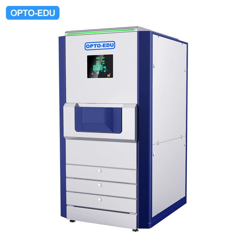
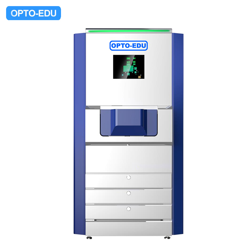
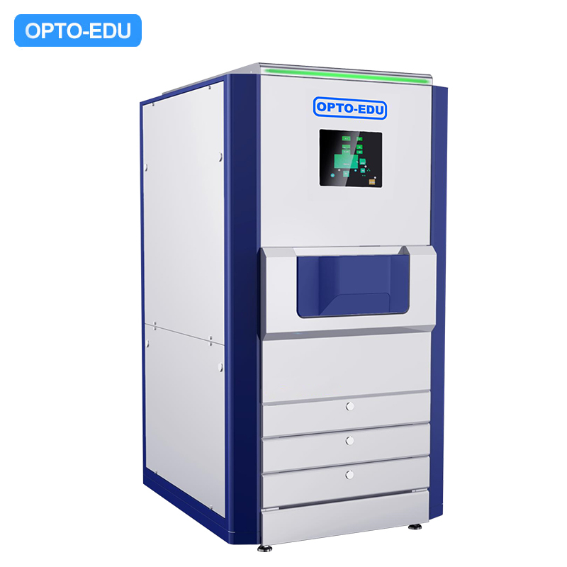
OPTO-EDU A63.7235 Yüksek Verimli Alan Emisyonlu Taramalı Elektron Mikroskobu 12KV 600000x
-
Vurgulamak
Alan Emisyonlu Taramalı Elektron Mikroskobu 12KV
,Yüksek Verimli Taramalı Mikroskop 600000x
,Yüksek büyütmeli OPTO-EDU SEM
-
Elektron silahıSchottky Tip Termal Alan Emisyon Elektron Kaynak Işın Akım Kararlılığı <%1/gün
-
Objektif lens sistemiSorril ™ Elektromanyetik Bileşik Lens Örnek Evre Yavaşlama Modu
-
standart çalışma mesafesi1.5 mm
-
Maksimum görüş alanı100um (standart çalışma mesafesi) 1mm (maksimum çalışma mesafesi)
-
Elektron Dedektörü (Standart)Sütun içi SE dedektörü lens içi BSE dedektörü
-
WD yükseklik tespitiFocus Tracking ™ Otomatik Odak İzleme Sistemi
-
Menşe yeriÇin
-
Marka adıCNOEC, OPTO-EDU
-
SertifikaCE, Rohs
-
Model numarasıA63.7230
-
belge
-
Min sipariş miktarı1 PC
-
FiyatFOB $1~1000, Depend on Order Quantity
-
Ambalaj bilgileriİhracat Taşımacılığı İçin Karton Ambalaj
-
Teslim süresi5~20 Gün
-
Ödeme koşullarıT/T, West Union, PayPal
-
Yetenek temini5000 Adet/Ay
OPTO-EDU A63.7235 Yüksek Verimli Alan Emisyonlu Taramalı Elektron Mikroskobu 12KV 600000x
Opto-EDU A63.7235 Yüksek verimli alan emisyon taraması elektron mikroskobu 12kv 600000x
Anahtar Özellikler
- Çözünürlük 1.5nm@1kv, otomatik edinme CM2 boyutuna kadar büyük görüntüyü dikiyor
- Her bir 100m piksel/s'de SE ve BSE'nin çift kanallı senkron görüntüleme
- Geleneksel elektron mikroskoplarının 10 katı kapsamlı görüntüleme hızı
- Masif SEM görüntülerinden hızlı bir şekilde veri analizi raporları
- Milimetreden nanometrelere çapraz ölçekli malzeme karakterizasyonu
A63.7235 yüksek verimli alan emisyon tarama elektron mikroskobu, araştırma ve endüstride yaygın olarak kullanılan çapraz ölçekli büyük ölçekli örnek SEM karakterizasyonu ve analizi için tasarlanmıştır. Otomatik ultra yüksek hızlı nano görüntüleme teknolojisi olağanüstü bir görüntüleme deneyimi sunar.
Temel yetenekler:
- Çözünürlük 1.5nm@1kv, otomatik edinme CM2 boyutuna kadar büyük görüntüyü dikiyor
- Her bir 100m piksel/s'de SE ve BSE'nin çift kanallı senkron görüntüleme
- Geleneksel elektron mikroskoplarının 10 katı kapsamlı görüntüleme hızı
- Masif SEM görüntülerinden hızlı bir şekilde veri analizi raporları
- Milimetreden nanometrelere çapraz ölçekli malzeme karakterizasyonu
Opto-EDU tarafından bağımsız olarak geliştirilen A63.7235 yüksek verimli alan emisyonu tarama elektron mikroskobu, görüntüleme teknolojisinde, hareket platformunda, devre kontrolü ve akıllı algoritmalarda sistematik yenilikçi tasarım yoluyla yüksek verimli görüntüleme elde etmektedir. Doğrudan elektron dedektörlerini benimser, geleneksel SEM teknolojisinin sınırlamalarını hız, doğruluk ve numune hasarıyla aşar.
Teknik Özellikler
| Elektron optik lens | |
|---|---|
| Elektron tabancası | Schottky Tip Termal Alan Emisyon Elektron Kaynak Işın Akım Kararlılığı <%1/gün |
| Objektif lens sistemi | Sorril ™ Elektromanyetik Bileşik Lens Örnek Evre Yavaşlama Modu |
| Çözünürlük | 1.5 nm @ 1kv 1.3nm @ 3kv |
| Daldırma elektromanyetik lens (*①) | |
| Hızlanma voltajı | 0.1-12 kV Sürekli ayarlanabilir (*②) |
| Büyütme | 500x ~ 600.000x (SEM görüntüsü) 1x-600x (optik navigasyon) |
| Işın akımı | 50pa ~ 30na (*③) |
| Standart çalışma mesafesi | 1.5 mm |
| Maksimum görüş alanı | 100um (standart çalışma mesafesi) 1mm (maksimum çalışma mesafesi) |
| Elektron Işın Blankarı | Elektrostatik boşluk |
Gelişmiş Özellikler
▶ Ultra hızlı görüntüleme
- Bağımsız geliştirilmiş donanım ve yazılım tasarımı yoluyla ikincil elektronların ve geri saçılmış elektronların çift kanallı senkron görüntülemesine ulaşıldı: Video seviyesi yüksek çözünürlüklü görüntüleme
- Yüksek tanımlı video seviyesi kare hızı, örnek dinamik değişikliklerin gerçek zamanlı gözlemlenmesini sağlar
▶ Yüksek görüntüleme kalitesi
- Benzersiz daldırma elektromanyetik bileşik lens sistemi optik sapmaları etkili bir şekilde azaltır
- Elektrostatik tarama sapma sistemi görüntü kenar bozulmasını azaltır
- Lens içi SE ve BSE yarı iletken doğrudan elektron dedektörleri, çift kanallı eşzamanlı yüksek hızlı görüntüleme etkinleştirir
- Aktif Tazminat Sistemi çevresel paraziti ortadan kaldırır
▶ Çapraz ölçekli büyük ölçekli görüntüleme
- Tam otomatik odaklama izleme sistemi ile ultra yüksek hızlı tarama görüntüleme özelliği
- AI görüntü işleme algoritmaları, yüksek çözünürlüklü tam otomatik kesintisiz matris taramasını etkinleştirir
- Büyük boyutlu nanometre düzeyinde çözünürlüklü panoramik görüntüleme elde etmek için otomatik olarak dikiş
▶ Akıllı analiz
- Büyük Veri Akıllı Analizi, Hızlı Veri Analizi Raporları Üretimi
- Akıllı görüntü işleme, özelleştirilmiş görüntü ölçümü, istatistik ve analiz
▶ Basit işlem
- Tam otomatik numune yükleme ve navigasyon, tek tıklamalı örnek değiştirme
- Geniş alan optik görüntüleme navigasyonu, SEM görüntüleme ile sorunsuz bir şekilde bağlanır
- 24/7 tam otomatik insansız çalışma özelliği
Uygulama Örnekleri
Hedef alan örneklerinde tam otomatik tarama yapmak için diziler taraması kullanarak tarama elektron mikroskopisi altında fare beyni, kalp, karaciğer ve böbrekteki hücrelerin mikro yapısını gözlemleyin.
Numune, sürekli bir dilimleme yöntemi kullanılarak, yüzlerce dilim toplayarak, bunları bir örnek daireye yerleştirerek ve aynı anda SEM'e yükleyerek hazırlanır.
Patolojik analiz: Tüm dilimle ilgili tüm ayrıntılı bilgileri kapsamlı bir şekilde toplayın ve böbrek dokusu üzerindeki hücre altı organel ultra yapısını açıkça gözlemlemek için herhangi bir alanda yakınlaştırın.
Notalar
* Not:
①: Ferromanyetik materyalleri gözlemlemek için isteğe bağlı inmersiyon olmayan elektromanyetik lens
②: İsteğe bağlı 0 ~ 30kV elektron tabancası
③: İsteğe bağlı 100na
④: İsteğe bağlı lazer interferometre
①: Ferromanyetik materyalleri gözlemlemek için isteğe bağlı inmersiyon olmayan elektromanyetik lens
②: İsteğe bağlı 0 ~ 30kV elektron tabancası
③: İsteğe bağlı 100na
④: İsteğe bağlı lazer interferometre
ilgili ürünler
Ürünlerimiz tüm dünyada satılmaktadır. Ürünlerimizin tüm sürecinden emin olabilirsiniz.